SC414/SC424
26
Applications Information (continued)
VOUT Plane
on Top layer
L
C
IN
CFF
RFB2
RFB1
RILIM
LX plane on inner
or bottom layer
All components
shown Top Side
AGND plane on
inner layer
V
IN
plane on inner
or bottom layer
RES_GND AGND connects
to PGND close to SC414/SC424
Pin 1 marking
SC414/SC424 with
vias for LX, AGND,
VIN
PGND on inner
or bottom layer
PGND
C
OUT
Note: This figure is not
to scale
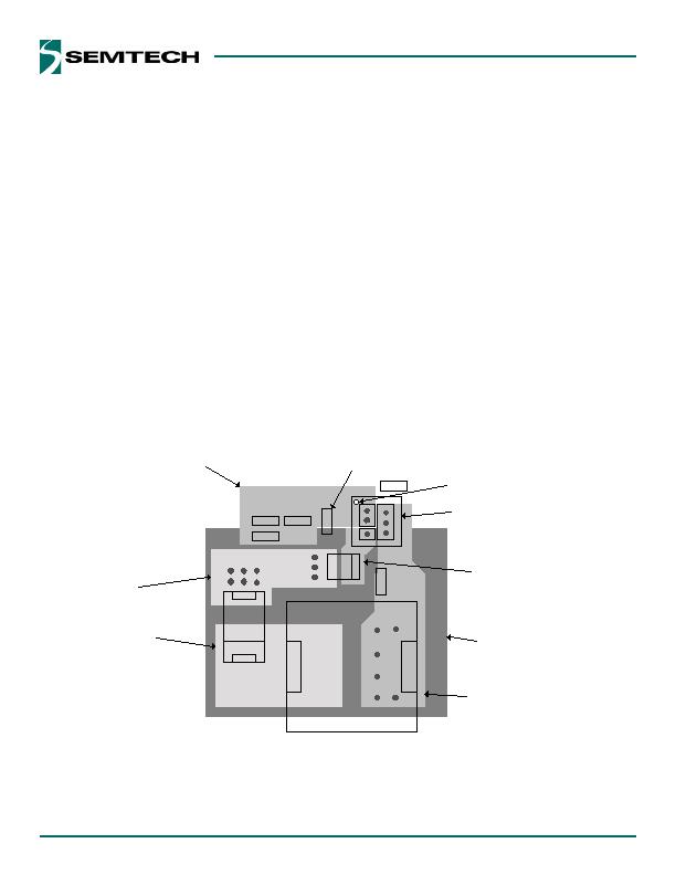
Figure 15 PCB Layout
The switching frequency also varies with load current as a
result of the power losses in the MOSFETs and the induc-
tor. For a conventional PWM constant-frequency con-
verter, as load increases the duty cycle also increases
slightly to compensate for IR and switching losses in the
MOSFETs and inductor. A constant on-time converter
must also compensate for the same losses by increasing
the effective duty cycle (more time is spent drawing
energy from V
IN
as losses increase). The on-time is essen-
tially constant for a given V
OUT
and V
IN
combination, to
off set the losses the off -time will tend to reduce slightly as
load increases. The net eff ect is that switching frequency
increases slightly with increasing load.
PCB Layout Guidelines
The optimum layout for the SC414/SC424 is shown in
Figure 15. This layout shows an integrated FET buck regu-
lator with a maximum current of 6A. The total PCB area is
approximately 20 x 25 mm.
Critical Layout Guidelines
The following critical layout guidelines must be followed
to ensure proper performance of the device.
IC Decoupling capacitors
PGND plane
AGND island
FB, VOUT, and other analog control signals
BST, ILIM, and LX
Capacitors and Current Loops
IC Decoupling Capacitors
A 0.1 糉 capacitor must be located as close as
possible to the IC and directly connected to pins
2 (V5V) and 3 (AGND).
"
"
"
"
"
"
"
发布紧急采购,3分钟左右您将得到回复。
相关PDF资料
SC4250LISTRT
IC HOT SWAP CTRLR 8-SOIC
SC427MLTRT
IC REG DL BUCK/LINEAR 32MLPQ
SE95D,112
IC SENSOR TEMP 2.8-5.5V SOT96-1
SE97BTP,547
IC TEMP SENSOR DIMM 8HWSON
SE98ATP,547
IC TEMP SENSOR DDR 8-HWSON
SG6901ASZ
IC PFC CTLR AVERAGE CURR 20SOIC
SG6932SZ
IC PFC CONTROLLER CCM 16SOP
SG6961SY
IC PFC CTRLR AVERAGE CURR 8SOIC
相关代理商/技术参数
SC4-25
制造商:JAMECO VALUEPRO 功能描述:CABLE,SHIELDED,4 CONDUCTOR,GRAY,24AWG,25 FEET,ROUND
SC4250
制造商:SEMTECH 制造商全称:Semtech Corporation 功能描述:Negative Voltage Hot Swap Controller
SC4250_05
制造商:SEMTECH 制造商全称:Semtech Corporation 功能描述:Negative Voltage Hot Swap Controller
SC4250HISTR
制造商:Semtech Corporation 功能描述:
SC4250HISTRT
制造商:Semtech Corporation 功能描述:Hot Swap Controller 1-CH -80V 8-Pin SOIC T/R
SC4250LISTR
制造商:SEMTECH 制造商全称:Semtech Corporation 功能描述:Negative Voltage Hot Swap Controller
SC4250LISTRT
功能描述:IC HOT SWAP CTRLR 8-SOIC RoHS:是 类别:集成电路 (IC) >> PMIC - 热交换 系列:- 产品培训模块:Lead (SnPb) Finish for COTS
Obsolescence Mitigation Program 标准包装:119 系列:- 类型:热交换控制器 应用:通用型,PCI Express? 内部开关:无 电流限制:- 电源电压:3.3V,12V 工作温度:-40°C ~ 85°C 安装类型:表面贴装 封装/外壳:80-TQFP 供应商设备封装:80-TQFP(12x12) 包装:托盘 产品目录页面:1423 (CN2011-ZH PDF)
SC4-26#
制造商:Vector Electronics & Technology Inc 功能描述:Screw, #4-40 x 3/4 inch, thread to HD